Using advanced CAE software,designer simulate the whole molding process with the computer and this will help us to reduce the times of trying mold die and to accelerate development cycle,and it can also optimize the molding process to help customer improve production.
For example,designer can get the effect when he modiifies the size of Runner,Gate,Cavity air vent and related parameters,and observe if any quality problems happen.Such as the Void,under fill Encapsulation,etc.
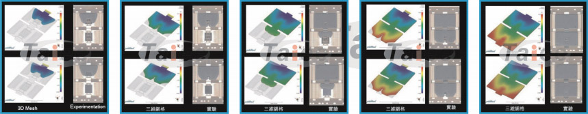
 Result analysis:During the filling process, the flow of EMC is very smooth and balanced, and the flow velocity of each cavity is roughly the same. The design of runner and gate is reasonable.
Autodesk Moldflow AMI2012 purpose:
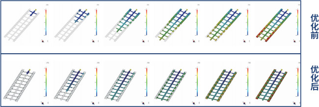
1.The molding conditions and filling mode of thermosetting materials were optimized( Comparison before and after optimization)
Result analysis:During the filling process, the flow of EMC is very smooth and balanced, and the flow velocity of each cavity is roughly the same. The design of runner and gate is reasonable.
Autodesk Moldflow AMI2012 purpose:
1.The molding conditions and filling mode of thermosetting materials were optimized( Comparison before and after optimization)
 2.Prediction of pressure and clamping force requirements;
 3.The wafer deformation prediction caused by the pressure difference between the upper and lower dies is calculated;
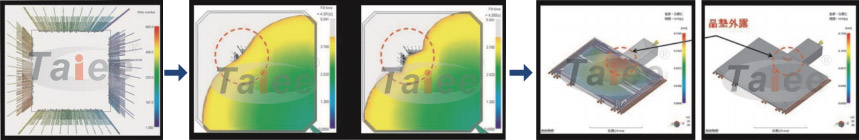
 4.To predict the offset effect caused by EMC flowing through the gold line;
5.Predict the location of exhaust and package products;
6.The deformation of package is predicted( For example, chip leakage)
7.Calculate that EMC is the least used.
4.To predict the offset effect caused by EMC flowing through the gold line;
5.Predict the location of exhaust and package products;
6.The deformation of package is predicted( For example, chip leakage)
7.Calculate that EMC is the least used.
 To simulate the process of TSOP package form:
1.Preparation for simulation
To simulate the process of TSOP package form:
1.Preparation for simulation
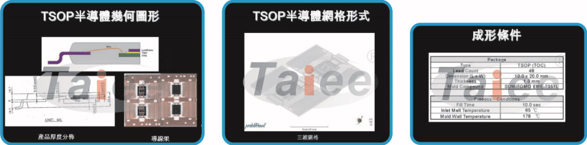 2.Package simulation process